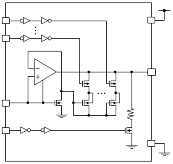
Service

Advantages from Experience
and Reliable Quality

Frontier Technology’s wide range of skills and experiences ensures timely and quality outputs.

Development Flowフロンティアテクノロジー

Development Tools

フロンティアテクノロジー

Development field

Consumer equipment

Printer/ MFP Projector Functional Watch Health care equipment
Wearable equipment LCD TV Game equipment

Automobile

Car navigation Car Audio Display Panel
LED head light ECU

Proven Developments

Front-end/Back-end

Macro

Menu : Oscillating circuit   Circuit Simulation Layout
kHz Bandwidth 32kHz Crystal oscillation
  CR Oscillating(40kHz~60kHz)
MHzBandwidth Crystal and ceramic oscillations(1MHz~40MHz)
  CR Oscillating(500kHz~12MHz)
GHz Bandwidth PLL(400MHz~1.3GHz)
Menu : Power circuit Circuit Simulation Layout
Charged pump system
PWM system
Rectification system
LDO
BGR
Menu : Others Circuit Simulation Layout
Reference constant current source circuit
Supply voltage detecting circuit
Solar charge control circuit
Oscillation stop detecting circuit
Power on reset circuit
Operational amplifier
ADC
DAC
LF
RF
LVDS
SLVS
Motor driver
Transceiver
I/O circuit
SRAM
Digital circuit
S/C Lib.
G/A Lib.

Chip

  Circuit Simulation Layout
Microcomputer  
Driver
Power supply
Battery protection
RF
USB
RTC
MEMS controller

Fab

Major domestic maker VIS (Vanguard)
TSMC Dongbu HiTek
UMC Samsung
Global-Foundry LFoundry
TowerJazz

Process

0.60um 2 layer metal 65nm 12 layer metal
0.35um 3 layer metal 55nm 8 layer metal
0.25um 3 layer metal 40nm 9 layer metal
0.18um 5 layer metal 28nm 7 layer metal
0.15um 5 layer metal

Design Example

基準生成回路

The details

Voltage Reference Generator Circuit

The detailsClose

  • 基準生成回路 フロンティアテクノロジー
  • 基準生成回路 フロンティアテクノロジー
About the circuit :

Voltage Reference Generator Circuit Summary

Summary

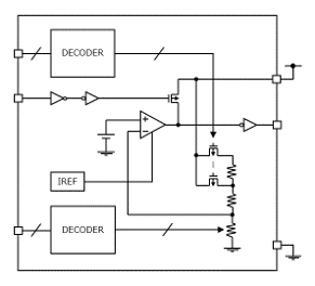
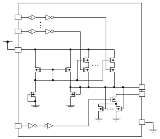
With a reference current source using a depression NMOS transistor, the circuit activates instantly when the power is turned on and generates reference voltage with NMOS bias transistor.

Application

Source of reference voltage to be supplied to the regulating amplifier.

Experience & Performance

Used in low power microcomputers.

Key Elements

Layout wires as GND shielding to output reference voltage while paying attention not to cause crosstalk with other signals. Main transistors have their current running in the same direction to improve the currents precision. Making geometry consistent enhances the characteristics.

定電圧生成回路

The details

Constant Voltage Generation Circuit

The detailsClose

  • 定電圧生成回路 フロンティアテクノロジー
  • 定電圧生成回路 フロンティアテクノロジー
About the circuit :

Constant Voltage Generation Circuit

Summary

By using power source voltage, the circuit generates constant voltage that is exclusively used for oscillating circuit. Current source of amplifier is supplied by voltage reference generator circuit.

Application

Source of constant voltage supplied to oscillating circuit.

Experience & Performance

Used in low power microcomputers.

Key Elements

Differential pairs of amplifier is located per Common Centroid. Tail current source of amplifier is generated in same direction and shape as that of NMOS transistor of voltage reference generator circuit to improve the current precision.

発振回路

The details

Oscillating Circuit

The detailsClose

  • 発振回路 フロンティアテクノロジー
  • 発振回路 フロンティアテクノロジー
About the circuit :

Oscillating Circuit

Summary

Having crystal unit attached, the circuit generates frequency of 32.768 kHz. Generated oscillation can be adjusted by digital control. Voltage source is supplied by constant voltage generator circuit.

Application

Low power RTC

Experience & Performance

Used in low power microcomputer.

Key Elements

Layout wires for gate/drain signals while paying attention not to cause crosstalk with other signals. Avoid laying out signals to be in parallel or crossed manners that may cause opposite phases.

電源電圧検出回路

The details

Power Supply Voltage Detection Circuit

The detailsClose

  • 電源電圧検出回路 フロンティアテクノロジー
  • 電源電圧検出回路 フロンティアテクノロジー
About the circuit :

Power Supply Voltage Detection Circuit

Summary

Detecting power supply voltage down. When power supply voltage has been dropped, it detects immediately and output.

Application

Mobile device which requires battery-powered.

Experience & Performance

Used in low power microcomputer.

Key Elements

Converter differential couple does routing of layout considered direction of flow and circuit patterns.
For preventing accident, dummy friction is allocated around partial pressure friction to stabilized friction per one unit.

A/Dコンバータ回路

The details

A/D Converter Circuit

The detailsClose

  • A/Dコンバータ回路 フロンティアテクノロジー
  • A/Dコンバータ回路 フロンティアテクノロジー
About the circuit :

A/D Converter Circuit

Summary

Output voltage at A/D converter is compared based on analog input voltage at a constant frequency by sample-hold circuit. Result are shown by digital code.

Application

Mobile device which requires battery-powered.

Experience & Performance

Installed for low power microcomputers.

Key Elements

Allocate capacitor array for common centroidal relation to minimize variation. Layout wires carefully while parasitic capacitance is weighted.
Dummy capacitance is allocated to minimize errors surround capacitor array. Unit will be stable by this method.